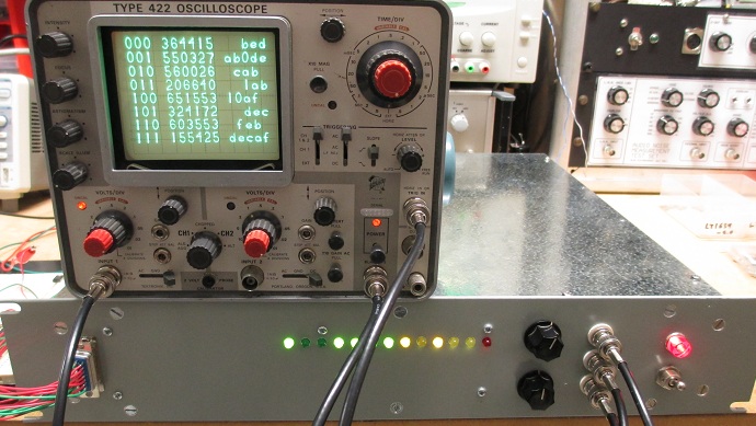

System introduction
This unit is an alphanumeric character generator which produces deflection and banking signals to trace out a display on an oscilloscope screen. The display produced consists of 128 programmable characters arranged in 8 rows of 16. The complete character set is comprised of the numbers 0 through 9 and the letters a through f, giving a total of 16 unique characters in addition to a blank space. The unit is therefore suitable for the display of computer data in hexadecimal format.A noteworthy aspect of the unit is that the character generation is based on analogue principles. The actual R.O.M., which effectively contains the data for tracing out each individual character, is in fact completely analogue. The characters are produced by a Fourier synthesis technique that I found outlined in an article entitled Generating Characters, published in the January 3rd, 1958 issue of ELECTRONICS, engineering edition.
The authors (from the Lincoln Laboratory of MIT) detail a demonstration unit for generating the Arabic octal numerals 0 through 7, synthesising the deflection waveforms for each character from artificially generated sine and cosine terms of 5 harmonic frequencies, with a reference frequency of 30 kHz. The system described displayed its eight numerals, 0 through 7, on the face of an oscilloscope CRT four rows deep, for 32 characters in total. The design was somewhat inflexible however, as the selection of a specific character in each of the 32 available locations was made in a hardwired diode matrix.
Reading through the article I was fascinated and immediately enamoured with the concept of Fourier synthesis for producing a display of alphanumeric characters, so much so that I just had to design and construct my own, practical and useful version. To provide a useful data display for my analog/hybrid and digital computer projects, I settled upon the expanded specification of a 16-character character set (plus bank space) displayed in 8 rows of 16. Rather than a hardwired diode matrix, the specific character displayed in each of the 128 avaliable locations is stored in a volatile static RAM (SRAM), which is remotely programmable through a 12-bit wide parallel port.
In common with the system described in the cited reference, my unit synthesizes each character from sine and cosine terms of 5 harmonics, but that is where most of the similarities in the practical circuit realisation end. In my implementation described here, each character is visibly traced out in six eighths of the 50 uS period of a 20 kHz fundamental reference. Remote programming of the display, through the parallel port, is asynchronous and by means of buffering and data transfers to the SRAM during blanking intervals only, does not produce glitches or visible interruption to the generated display. The manner in which all of this is achieved, by means of simple, discrete 74-series logic circuitry, is detailed in the following paragraphs.
But firstly, here is a brief demonstration video of the unit in operation:
An operational outline of the display control logic
The blanking interval mentioned in the system introduction is two eighths of a period, or 12.5 us, in duration, comprised of 6.25 uS at the end of one complete period and 6.25 uS at the start of the immediately next period, during which the beam of the cathode ray tube is cut-off. This period of time is that between the complete visible tracing out of one character to the next, during which the beam of the cathode ray tube is invisibly manoeuvred in position from the end point of one traced out character to the starting point of the next. These timing intervals are illustrated in Figure 1, showing the actual synthesized X (horizontal) and Y (vertical) deflection waveforms necessary for scribing the numeric character 2 onto a cathode ray tube face, in relation to the blanking interval, or Z-modulation, waveform.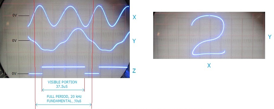
Figure 1 - synthesized waveforms for generating a character
Remote programming is very simple. The first 7 bits of the 12-bit wide programming word (designated A0 through A6), applied to the parallel programming port, are the SRAM address bits which select the character position (0 through 127decimal) to be set. The remaining 5 bits of the programming word (designated D0 through D4) are the SRAM data bits, which select the actual character to be displayed in the nominated (addressed) position. The data value, in the range of 0 through Fhex, corresponds directly to the alphanumeric character to be displayed. For example, a data value of 7 displays 7, while a data value of Ehex displays e. While only 4 data bits (D0 through D3) are required to select any one of the 16 available characters to be displayed, the 5th and final data bit is required to select a blank space. When the 5th data bit (D4) is high, no character will be displayed in the addressed position, irrespective of the logic state of bits D0 through D3. A blank space is not a R.O.M.-generated character as such when D4 is programmed high for a given character position, the blanking interval for that position is simply extended to the full 50 uS period.
So then, partially reiterating, the process of programming a character of the display involves applying the correct address and data values simultaneously to the 12-bit wide programming port. The final step is to assert the single control line, designated WRITE. However, as mentioned previously, programming is asynchronous, so there are therefore a few necessary requirements and restrictions.
The control logic ignores the status of the WRITE pin during the 12.5 uS blanking intervals. The WRITE pin must therefore be asserted (pulled high) for a duration (by at least a couple of uS) greater than 12.5 uS. The 12-bits of data presented to the programming port must of course be stable during this complete period.
Holding the WRITE pin high for greater than 12.5 uS ensures that even if the occurrence is partially coincident with a blanking interval, the WRITE status will always be gated through by the control logic - if coincident with a blanking interval, than either immediately prior to, immediately after, or both. When a WRITE strobe is passed, an edge-triggered monostable circuit generates an internal write pulse for the internal 12-bit data latch, writing and storing the 12-bits presented to the programming port into this effective memory. From this point onwards, the status of the programming port pins no longer matters and the WRITE pin logic state may return low. A convenient WRITE pin strobe duration is 15uS.
Approximately half way through the next subsequent blanking interval the contents of the data latch is automatically and seamlessly transferred to the SRAM by the control logic. The 7 address bits (A0 through A6) directly address the SRAM, while the 5 data bits (D0 through D4) are written into the addressed location. A programming cycle for a single character position is now complete. With this sequence of events now detailed, it should be clear that programming cycles cannot occur at repetition rates greater than 50 uS. However this is not much of a limitation, concerning dynamics of the generated display. For example WRITE strobes at a repetition rate of 60 uS permits the entire 128 displayed characters to be programmed or updated in less than 8 mS faster than the blink of an eye.
Generating the sine and cosine reference terms
As the X and Y deflection waveforms required to scribe each unique character are synthesized from five harmonics having a fundamental frequency of 20 kHz, an amplitude-stable reference of these 5 harmonic frequencies, both sine and cosine terms, plus the inverses, must the generated. A total of twenty 1V peak reference sinusoids are generated, tabulated thus:Term Harmonic# Frequency (kHz) Phase (degrees) sin wt 1 20 0 -sin wt 1 20 -180 cos wt 1 20 +90 -cos wt 1 20 -90 sin 2 wt 2 40 0 -sin 2 wt 2 40 -180 cos 2 wt 2 40 +90 -cos 2 wt 2 40 -90 sin 3 wt 3 60 0 -sin 3 wt 3 60 -180 cos 3 wt 3 60 +90 -cos 3 wt 3 60 -90 sin 4 wt 4 80 0 -sin 4 wt 4 80 -180 cos 4 wt 4 80 +90 -cos 4 wt 4 80 -90 sin 5 wt 5 100 0 -sin 5 wt 5 100 -180 cos 5 wt 5 100 +90 -cos 5 wt 5 100 -90By means of a combination of band-pass filtering, all-pass filtering and inversion, these twenty reference sinusoids are all produced from five reference square waves, of 20, 40, 60, 80 and 100 kHz. These square waves, having the correct phase relationships with respect to each other, are all derived from a single, master crystal clock source, by combination of synchronised digital division and phase-locked-loop-based multiplication. The square waves are generated on the PCB entitled the "Logic" board. An oscilloscope screen photo of the five square waves, displayed simultaneoulsy, is shown in Figure 2.
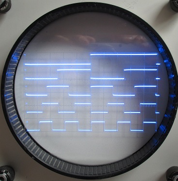
Figure 2
Ripple counter U4 and quad NAND gate U5 form in combination a divide-by-5 counter, dividing the 800 kHz reference to 160 kHz, which is divided further again by the first three stages of ripple counter U6, which produces in succession the 4th, 2nd and 1st (fundamental) harmonic reference square waves of 80 kHz, 40 kHz and 20 kHz. NAND gates U7C, U7D and U8A through U8D produce a brief pulse on each falling edge of the 20 kHz square wave. This pulse is used to reset ripple counter U3, effectively locking the phase of the 100 kHz reference square wave into synchronisation with all of the others others.
The generation of the 3rd harmonic reference square wave is a little trickier. Unlike the other harmonic frequencies, 60 kHz cannot be derived from the 800 kHz reference by integer division, as 60 does not divide evenly into 800. However, all harmonics must ultimately be derived from the common reference to maintain the correct, locked-in phase relationships. The 3rd harmonic frequency is generated by multiplying the 20 kHz fundamental by 3. Ripple counter U10, in conjunction with quad NAND gate U11, forms a fixed divide-by-3 loop divider for phase locked loop U9. The VCO of U9 therefore oscillates at 3 times the reference frequency of 20 kHz.
The 5 reference square waves are routed to header P3, off the Logic board, for further processing on the Sine and Cosine Filter board.
All five harmonic frequencies are processed on the Filter board in an identical manner. Therefore, only the signal path of the fundamental frequency processing will be detailed. With reference to the schematic diagram of the Filter board, the 20 kHz square wave is first passed through two cascaded multiple-feedback bandpass (MFB) filter stages based on op-amps U1A and U1B. Each MFB filter stage has a Q of 4, a passband gain of unity, and is tuned to resonance by trimmer potentiometers RV1 and RV2 respectively. The MFB filter has zero phaseshift at resonance. Each MFB filter is tuned to the fundamental frequency of the square wave, attenuating the harmonic components to produce a clean sinusoid, in phase with the unprocessed square wave, at the output, pin 7, of U1B.
Note that as shown in Figure 2, the generated and phase-locked reference square waves all have a common, coincident falling, rather than rising, edge. The square waves are therefore the inverse terms of the harmonic frequencies. The sinusoid thus produced at the output of U1B is therefore sin wt. This sinusoid is amplitude scaled to 1V peak by the inverting amplifier stage U1C. Trimmer potentiometer RV3 is provided for amplitude calibration. Due to the signal inversion, the scaled signal at the output of U1C is now sin wt.
An inverting, unity-gain all-pass filter based on op-amp U1D produces the phase-shifted -cos wt term from the sin wt term. Trimmer potentiometer RV4 is provided for calibration of the 90 degree phase-shift. The signals are routed to header P2, off the Filter board to the R.O.M board. The Filter board therefore produces all of the required sin n wt harmonics terms and all of the cos n wt harmonic terms. These ten waveforms are all shown in the cathode ray oscilloscope screen photos of Figure 3.
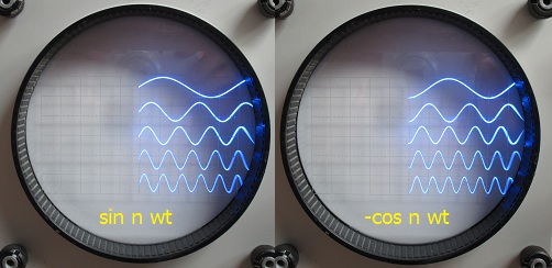
Figure 3
Character generation by the Fourier R.O.M.
The sixteen complementary X and Y deflection signals required to scribe each of the sixteen individual alphanumeric characters are finally assembled from the reference terms on the R.O.M board. The R.O.M. board is therefore, essentially, a hard-wired read-only memory, containing the unique Fourier component composition for each deflection waveform.The sin n wt and -cos n wt term signals from the Filter board are routed into the R.O.M. board through header P1 and buffered by op-amps U1 through U5 B & C, wired as unity gain voltage followers. Unity gain inverting stages based on op-amps U1 through U5 A & D finally produce the -sin n wt and cos n wt terms.
Each unique deflection waveform is synthesized by simply passively summing, with resistors, the required Fourier components at the required amplitudes. The DC terms, either positive or negative, where necessary, are also passively summed and combined. The synthesized deflection waveforms are finally buffered by op-amps U6 through U13, A though D, wired as unity gain voltage followers, and routed off to the Deflection board via headers P2 through P5. The Deflection board contains a pair of 1-of-16 multiplexers, addressed together by the data stored in the SRAM, to automatically select the synthesized X and Y waveforms for each specific character being scribed onto the CRT display at any given instant.
It probably doesnt need to be said that figuring out the Fourier components values for each character, and thus the resistor values of the R.O.M. board, was a particularly tedious and laborious task. Each character was first traced out on to graph paper. As a periodic waveform is a closed function, once the character was manually scribed, the curve had to be closed by a segment of a length commensurate in proportion with the time of the blanking interval to the net 50 uS period. This was achieved by measuring the total length of the visible portion of the characters curve with a length of string. The string was then cut down in length to the correct proportion (six eighths visible to two eighths blanked) and then used as an aide to trace out the segment length closing the curve.
A number of evenly spaced points, numbering approximately 40, were then plotted along the closed curve and the X and Y Cartesian coordinates values for each point tabulated. The numbered points, starting at 0, begin and end in the middle of the segment length added to close the curve. The tabulated X and Y values were then transferred into an Excel spreadsheet and the X and Y deflection waveforms reconstructed from these values respectively. The spreadsheet was also used to compute the Fourier coefficient values and the DC terms.
Deflection board
Referring to the Deflection board schematic, ICs U1 through U5 are wired to form the pair of 1-of-16 multiplexers. The multiplexers are addressed by data bits D0 through D3 of the SRAM, U18, which resides on the Logic board. The data lines are routed to the multiplexer via header P4 on the logic board and header P5 on the Deflection board.The X and Y deflection waveforms for the specific character selected by the multiplexer are present at pins 8 and 9 of U5 of the Deflection board respectively. These signals are buffered by unity gain voltage followers U6A and U6B, and then passed, via potentiometer pair RV1 and RV2, to inverting summing amplifier stages based on op-amps U7A and U8A respectively. The potentiometers permit the width and height of the displayed characters to be varied independently, to user preference.
Summing amplifiers U7A and U8A combine the synthesized deflection waveforms with stepped staircase waveforms, derived from the SRAMs 7-bit address counter. The staircase waveforms determine the position of each character on the display. The 7-bit address counter, U16, resides on the Logic board. U16 addresses the SRAM, U18, via tri-state buffer U17. The 7 address bits from the address counter are routed to header P6 of the deflection board via header P1 of the Logic board.
The 4 least significant bits of the address counter are decoded by a 4-bit R-2R DAC comprised of resistors R6 through R13. This produces a unipolar (positive) staircase waveform with 16 steps. Each step represents a character position in a horizontal row of characters. The address counter U16, of the logic board, is clocked on the negative edge of the 20 kHz fundamental reference waveform - as a consequence the character position count advances on each sucessive 50 uS period during which a complete character is scribed. The horizontal-positioning staircase waveform is consequently summed with the synthesized X deflection waveform. Resistor R21 injects a DC current into the summing junction of op-amp U7A for the purpose of DC level shifting, causing the constructed deflection waveform at the output of U7A to be become bipolar, effectively centred about 0V.
The 8 character rows are counted by the 3 most significant bits of the address counter, and decoded by the 3-bit R-2R DAC comprised of R14 through R19 and inverting logic gates U10A through U10C. The resultant waveform has 8 discrete steps; each step representing the vertical position of a character displayed. The vertical deflection signal is constructed by summing amplifier U8A in a manner identical to that of the horizontal deflection signal by summing amplifier U7A.
Op-amps U9 A through D and associated components form a pair of non-synchronised, ultra-low frequency triangle waveform oscillators, which serve a phosphor saver function. The triangle waveforms are separately summed in a small amount with the X and Y deflection waveforms by summing amplifier stages U7B and U8B. This causes the position of the display produced on the face of the CRT to slowly, but continuously and seemingly randomly, shift around by a small deflection factor on both the horizontal and vertical axes. As a consequence, no potentially unchanging character is ever permanently fixed to a single position. This lessens the likelihood of the phenomenon of phosphor burn damage to the CRT from occuring.
The deflection signals from the output pins of op-amps U7B and U8B are finally routed to the BNC signal-output jacks on the front panel of the unit via header P7. An oscillograph of these deflection waveforms is shown in figure 4.
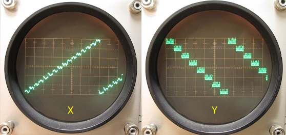
Figure 4
Interface board
The parallel programming port, accessible on the front panel of the unit via a female DB15 connector, is routed to the Logic board via the Interface board. The programming port inputs to the Logic board comprised of the 7 address, 5 data and single WRITE line, are all TTL-level compatible. The interface board provides transient over-voltage protection to all logic inputs by means of clamp diodes D1 through D27 in conjunction with current limiting resistors RP1 and RP2. LED indication of the logic state of all 13 lines is also provided. The WRITE pin pulse is stretched by monostable U3A, for reliable visual indication of the presence of WRITE enables on indicator LED 13.In conclusion
The fifth and last printed circuit board of which the system is comprised is the power supply board, however I do not feel that this requires much of a technical explanation. As shown in the photograph immediately below, I assembled and wired the complete unit into a homemade 2U relay rack case. The front panel is a pre-painted, 3mm thick, off-the-shelf blank made by Hammond Manufacturing. The case is constructed from 0.7mm thick galvanized sheet steel and 10mm X 10mm square aluminium stock, drilled and tapped for M4 assembly screws. The electrical interconnections between all of the circuit boards, front panel jacks and controls, etc, is detailed in the Wiring diagram.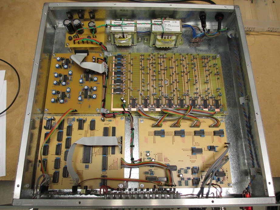
These are the 1nF capacitors for the MFB and all-pass filter stages. I originally loaded the green cap capacitors because that is what I had handy at the time, but that turned out to be a mistake. Firing up the character generator first thing on a cold winters morning, when it was only seven or eight or so degrees Celsius in my electronics workshop, I noticed that the displayed characters looked a little bit different to what they did once the heater warmed the workshop up to a more cosy 26 degrees or so.
Simply put, the ubiquitous green caps that I had installed had a terribly bad temperature coefficient, resulting in a small, but not insignificant temperature-dependent variation to the calibrated phases of the generated reference terms. Substituting with COG ceramic types, having a specified worse case temperature coefficient of +/-30ppm, completely solved the problem.