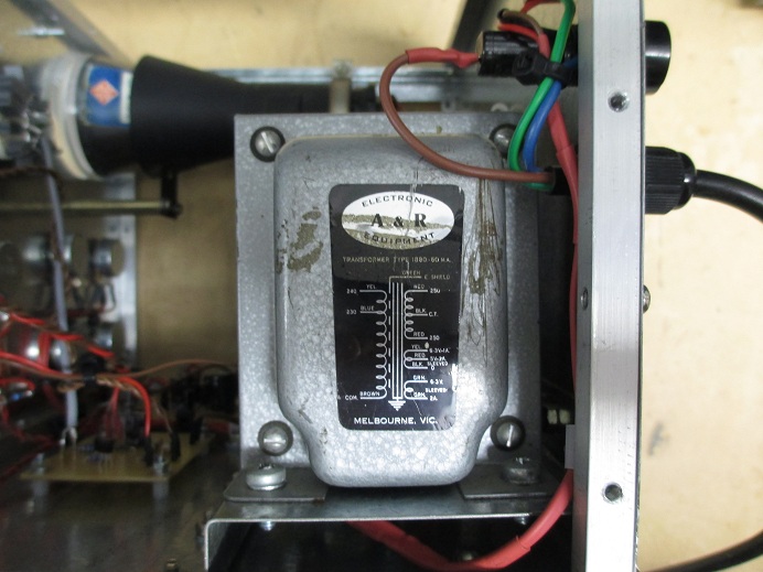
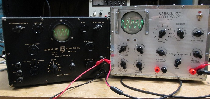
I had an itch to make use of one of my DG7-32 cathode ray tubes, from a collection of several sitting on a shelf. I also had an old vacuum-tube-era A&R-brand power transformer sitting in my junk box, which I handily noted provides all of the voltages required to implement a little CRO with said CRT, so thats, as I guess is wholly evident by now, exactly what I did.
The goal here, just for the sake of it, was to devise of an audio-bandwidth oscilloscope to a specification with the bare minimum number of components. To arrive at said specification I took inspiration from my 1940s model TA155 Philips oscilloscope, a unit which I own and have restored to working order and am, admittedly, quite fond of.
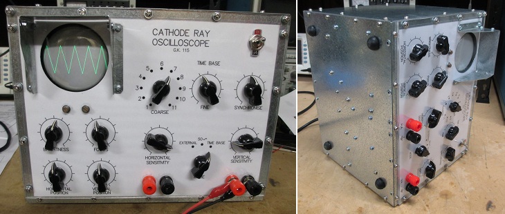
Except for some minor deviation the solid-state oscilloscope described here is functionally the same as the vacuum tube TA155. Pictured immediately below are the two oscilloscopes side by side, both displaying the same 1 kHz sinewave, operating in synchronised, linear-sweep time base mode.
External
50 Hz ~
Time base
In the External position, the horizontal deflection signal is taken from the horizontal input binding posts; the oscilloscope operates in X-Y mode, suitable for the display of Lissajous Curves or the like.
In the 50 Hz ~ position the input to the horizontal channel is taken from a 6.3 Vac winding on the power transformer, which has one end grounded. According to the operators manual for the Philips TA155, This is useful for identifying low frequency signals, such as amplifier hum, which are applied to the vertical amplifier input. If the frequency of this signal is 50 c/sec., an ellipse is formed on the screen."
In the Time base position the horizontal amplifier input is taken from the linear ramp/sweep waveform output of the time base oscillator circuit. The time base oscillator is of the simple injection-locked, rather than triggered, sort. In combination with the Synchronisation potentiometer, frequency and phase synchronisation of the time base to the vertical deflection signal is achieved by adjusting the time base Coarse and Fine frequency controls so that the time base free-running frequency of oscillation is roughly equal to the vertical deflection signal frequency, or less than by an even multiple; for example either one half, one third or one quarter the vertical deflection signal frequency. The position of the Synchronisation control will determine how finely the time base frequency controls will need to be adjusted to achieve a steady and stable lock.
Here is a demonstration video showing the oscilloscope operation in Time base mode, the time base at various frequency settings being successfully synchronised to the displayed vertical input signal (a 1 kHz triangle wave):
Circuit description
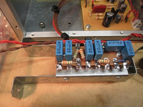
Now if you havent already peeked at the schematic diagram you might be wondering just how much solid-state componentry went into the implementation of all this amazing functionality? Well the answer is a grand total of six silicon transistors and two silicon diodes! With reference to the schematic diagram each defection amplifier is an ac-coupled long-tail pair; QA1/ QA2 and QA3/QA4, located on the Amplifier printed circuit board. The signal input for each amplifier is taken in single-ended fashion from its respective sensitivity potentiometer (RV1 and RV2) while the differential collector signal pair drives the respective deflection plate pair of the cathode ray tube.
The time base sweep generator is an R-C (resistor-capacitor) relaxation oscillator based on a programmable unijunction transistor (PUT), QT1 (located on the Time base printed circuit board). The linear ramp waveform developed across the timing capacitor is buffered by emitter-follower QT2 to preserve its linearity. Technically speaking, the 2N6027 PUT more closely resembles a thyristor than a transistor, but given the established nomenclature I feel at liberty to declare this a six-transistor scope!
The timing capacitor of the PUT relaxation oscillator is charged via Fine frequency control potentiometer RV4 in series with RT5, from a potential of a little less than 40V. PUT QT1 fires when the voltage at the anode exceeds the potential at the gate by one silicon diode drop (about 0.7V). The gate is held at a nominal potential of just under 6V by potential divider resistors RT3 and RT4. Since this potential is small relative to 40V the ramp waveform developed across the timing capacitor is reasonably linear. The linearity isnt perfect, but it isnt easy to spot on the face of a small cathode ray tube not equipped with a graticule. For the sake of simplicity there is no blanking of the horizontal sweep re-trace as such, but the fast re-trace typically isnt visible for the most part unless the display brightness control is turned up high - see the demonstration video above.
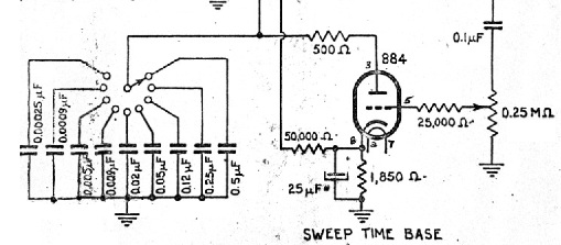
My PUT time base design was inspired by that of the TA155 oscilloscope, which, rather than a PUT, utilises a type 884 thyratron tube to perform essentially the exact same function:
My PUT time base design is synchronised in an equivalent manner. A proportion of the vertical deflection signal (ac-coupled by capacitor CA5 from the collector of transistor QA2 on the Amplifier PCB), via the Synchronisation potentiometer (RV3) is permitted to modulate the gate potential of the PUT. I think it's quite neat that a semiconductor device exists which enables the thyratron time base circuit to be replicated in solid-state in such a closely equivalent manner, and this was a significant motivational factor in this projects realisation. Though I think that the days of the PUT may be numbered. On Semiconductor was the last major manufacturer to produce the 2N6027 (and 2N6028) but they have since ceased production, declaring the device obsolete. At the time of writing (September 2016) Central Semiconductor Corp. is the only remaining producer of the 2N6027 and 2N6028 (in both through-hole and surface mount package variants) that I am aware of.
All of the oscilloscopes circuitry is powered from symmetrical rails of approximately +/-350V, derived from the 500V, center-tapped secondary winding of the power transformer. DP1 and DP2 on the power supply printed circuit board are half-wave rectifiers and capacitors CP1 and CP2 are the respective filter capacitors.
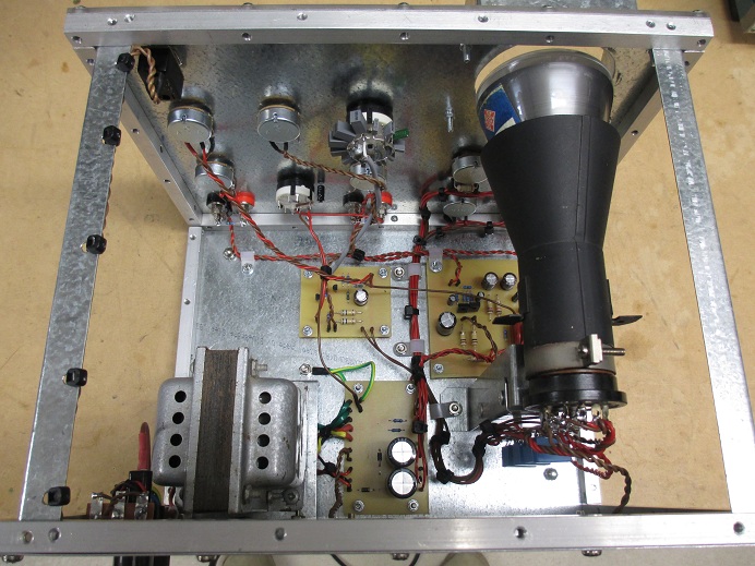
Well, this was a rather simple project from an electrical perspective, so I fell that Ive elaborated upon the technical design to an adequate degree of detail. Ill now close the exposition of this little project simply with some photographs of the insides of the completed product: